2012-06-21 PCB; foredrag og praktisk
et lille introduktionskursus i hvordan men simpelt med få midler kan få lavet et PCB til sine små projekter
kurset formål er at lære alle interesserede og ivrige HAL9K-medlemmer selv at kunne lave PCB til fritid
næste gang Dato : 21 Juni 2012
sted : Rapsgade 1, AALBORG 9000
hvem kan deltage : alle HAL9K medlemmer og interesserede.
tovholder og tilmelding: Ivan Holm på Discos-listen
wiki kan ses herunder
Printed circuit board
- What is Printed circuit board (PCB)
- How to create PCB Footpront and Circuit
- Where to get stuff
- How to make PCB
- SMD
- Literature
What is Printed circuit board (PCB)
Print Circuit Board is to make electronic more easy to handle electronic component at one place and often referred to abbreviation to PCB (Printed circuit board). They are made by an isolator and copper or aluminum 99.99% it is copper it is used sometime with soldering tin surface
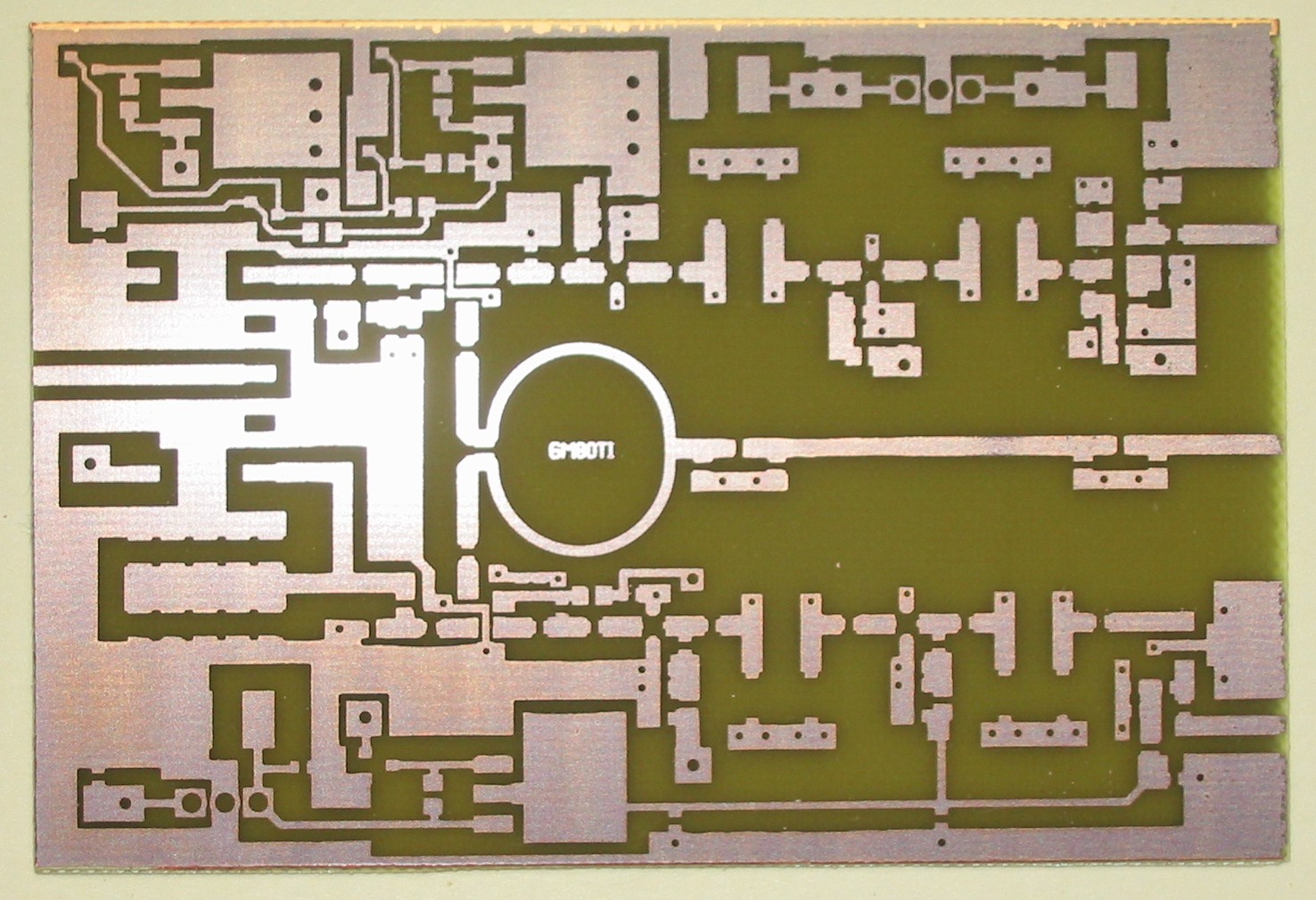
 this is an copper PCB layout.
 an ALU print with silkscreen
the copper Print is the most non resistance and cheapest compared to other non resistance material and lead heat that why 99.99% is copper PCB. but why does some use ALU PCB the reason for this is that ALU is good as an cooling that why many Power-Led PCB or others with heat component use ALU to transfer Heat away.
PCB link :
SMD PCB mount
PCB Design & Layout Tutorial by David Jones
How to create PCB Footprint and Circuit
When you want to make your own PCB if you not wont to drew it in freehand by an PCB-Pen you need some software to handle the component package and layout net/part-list also further. There are many PCB tool software to do this.
Here are some, but otherwise just Google “PCB Tool software”. Some are free, some are open-source and some are only trial versions and only buy version with support. some most used by private is a List down here.
- Eagle Cad PCB “demo for free with limit” (Win + Linux+ mac OS x) Eagle
sparkfun has a demo how to create create schematic and PCB schematic and PCB even your own component New Part in Eagle PCB program
- Kicad PCB “open-source” (Win + Linux + Mac) Wiki & Kicad homepage
- gEDA suite “open-source” (*nix + Linux + OS X + Windows) Wikipedia gEDA suite
- Diptrace “free version limit to 200 netlist line between component” (Win + other???) Diptrace homepage Visio studio appearance
- ORCAD DEMO free version ORCAD DemoLimitations are in the size and complexity of the design.
- PCB123 Free see some turtual on youtube PCB123
Where to get stuff
A few companies that have solder or PCB in Denmark
elektronik-lavprisÅrhus + shop
let-elektronik Aalborg after appointment
El-supply in Nexø Bornholm only web
RC-Vejle in Vejle only web
Brinck in Copenhagen + shop
j-solutions.dkonly webshop
Others…
How to make PCB
Starting with a board with a opaque (full covered) metal layer, from where the undesired metal is removed, typically by etching.
- Ironing toner on to PCB The Danish version and the English version Note if you are making only the pcb for SMD layer (soldering layer). You have to mirror the PCB otherwise the through hole layer (component Layer) do not mirror.
- Others method with toner transfer vacuum hot transfer
- Manual application on photo-PCB Drawing in freehand directly on your PCB With special PCB-Pen. sometimes it is more easy to drill holes in the print you can follow
- Others… (mechanical removal)
How to solder
The soldering are some correct way to solder and very Many Bad way to do soldering. this video How To Solder video I recommend to see
- Solder Remember all solder Iron are Hot do not burn yourself
- Solder tin solder-tin is made by Tin in shape of an tube and in this tube there is some chemical that make the tin soft and fragile when these chemicals disappears it get hard as normally tin. solder-tin contain some Flux that only purpose is to clean the surface and tin while soldering. others stuff is resin is to get the solder-tin to Hardness. solder-tin Wiki or solder Wiki chemical cant find the picture of inside the solder-tin but it can have more then 5 channels inside the solder-tin
 Remember all solder Iron are Hot do not burn yourself
- Soldering pasta can come in many different containers and if you do it by hand an
 will preferred but if you in industry where it make series production they will use larger containers. soldering-pasta is not soldering with an iron but with some Heat air flow like an oven or reworks-station here are some
- Other…
Remember all solder Iron are Hot do not burn yourself
- Solder Iron solder Iron is the basic Tool you must have if your going to do some electronic. There are many different solder-machine depending what you will use it for. the rule of Thom in this case is that the Iron Watt and size shot not sink many degrees in temperature when you are soldering….. it's recruitment that the soldering-tip is equal to 10% more size then the PCB-Pad depending on what your soldering on the temperature shut be near 325-350 Celsius. solder-tip
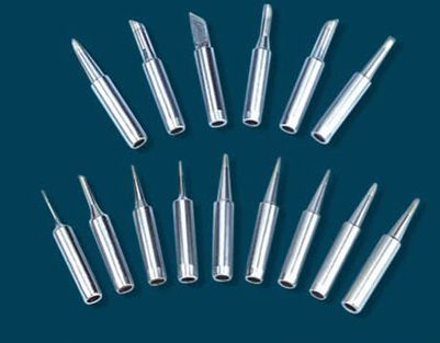 soldering tip for PCB and many others, is a good thing to have at tip with a flat surface, so they have more thermal contact with the copper and component
solder-station –> Rework-station –>
 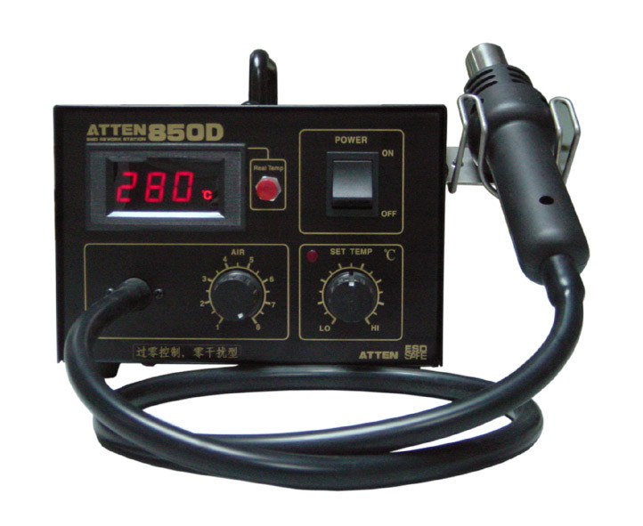 often used when you use solder-pasta
- Flux is as cleaning for oxidation and is a acid and that shot be cleaned with Isotropy-alcohol so it do not destroys the PCB and the component on the PCB
 soldering with Flux Flux soldering
SMD
SMD stand for [Surface Mounted Devise] “as I say (Små Mange Dimser)” and is what it says surface mounted component that do not need pin holes that why it is easy to make PCB for SMD because you do not need an drill if you make a simple PCB design. More info at All SMD wiki
 A few different sizes and components
- Resistor
Resistance all see under SMD
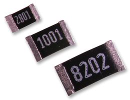
lookup datasheet
- Capacitor
ceramic 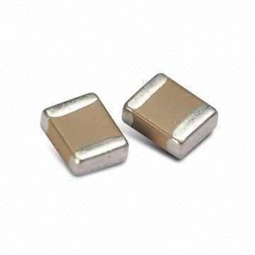
Bipolar  or
or 
lookup datasheet
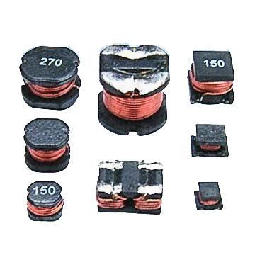
- Coil
- Diode
 or
or  or
or  or
or 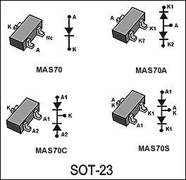 or others lookup datasheet
- Transistors other driver
- IC package
Literature
Downloads
Guide
Dansk versionENG version PCB transfer Iron and
Like Iron
photo PCB Dansk ENG version is on Youtube
ALL PCB to Mount
Schematic and
PCB Design and New Part to Eagle CAD PCB
Remember all solder Iron are Hot do not burn yourself
SMD PCB mount
IC package
SMD Code
WIKI
Video
PCB
PCB Design & Layout Tutorial by David Jones
photoprint transfer
Photo PCB
Inkjet PCB
InkJet PCB Rock
Pen Plotter
Photo PCB make your own. It is excessive
Silk Print
Dobbelt side PCB remember to be presize and to solder on both side the tin does not goes through holes unless you do some PCB Through Hole
Iron transfer Make Magazine video
SMT LINE SMT Production line EEVBLOG video
solder
Remember all solder Iron are Hot do not burn yourself
Q-Soldering
How to solder
SMD solder pasta
Flux soldering
SolderIron tips things to void
Tool
Remember all solder Iron are Hot do not burn yourself
reworks-station
Digital Soldering Iron
Wave-Soldering


